Tuesday, July 27, 2010

The Apple-1 "Garage" 2066 Crist Drive


On Friday July 23, 2010 I went to Los Altos with my brother and we stopped by 2066 Crist Drive which is where the Apple-1 printed circuit boards were stuffed with chips, and tested. This isn't where the hand-wired Apple-1 was built, that happened down the road in Woz's apartment, and he worked on it alone. This is where Steve Jobs used to live. For me it was somewhat surreal, as I live 3000+ miles from Crist Drive.

UPDATE from Woz received on Aug 04, 2010:

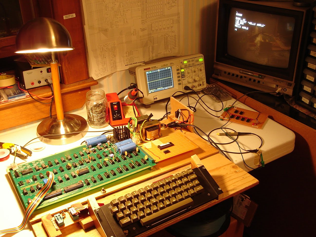
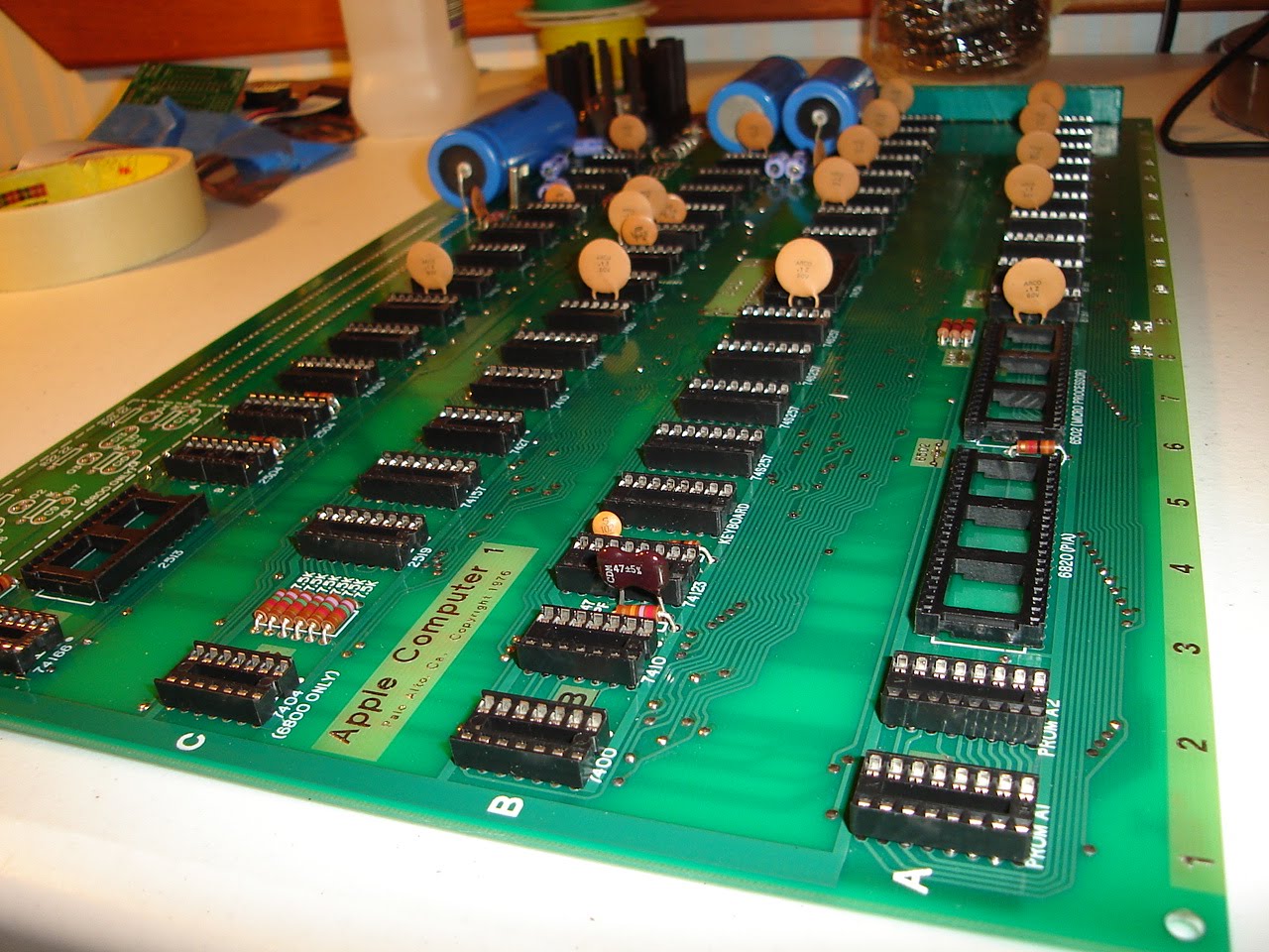
"The Apple I boards were manufactured and populated with components (sockets for the chips) and wave soldered at some company in Santa Clara. Those boards were driven to the house, and later the garage, where we inserted the chips and tested them. We did no soldering there.

My development work was all done in my apartment in the Villa Serra complex on Homestead Road, between Mary and Stelling. Also, much was done in my cubicle at HP's calculator division (APD) which was then in Cupertino, on Pruneridge Avenue (19925?) slightly East of Wolfe Road."


Saturday, June 26, 2010

Gold Purple Ceramic chips from 1976


I picked up a few (about 22) NOS gold ceramic DRAM and two 6820 chips recently. Here they are on an Obtronix board where I tested them. Out of the two 6820s, one doesn't work. The DRAM chips appear to work. These chips will eventually live on the Apple-1 Mimeo that I recently built.
The DRAM chips are MOSTEK 4027 P-3, most made in the 14th, and 19th weeks of 1976. The Motorola 6820L was made in the 48th week of 1976. Note the gold grounding straps on some of the DRAM chips.

Wednesday, June 2, 2010

Hand Wired / Wire wrapped Apple-1 = WOW


My friend Aurelien Zavattiero sent me these images earlier this week. He has spent the last 5 months working on a wire wrapped Apple-1 from scratch! Look at this, it's a work of beauty!
Aurel is very close to having the video section working as you can see in the images.

Monday, May 31, 2010

A1-Mimeo clone up and running (BASIC)

Apple-1 (Mimeo) Clone with the BASIC firmware card attached, shows the BASIC up and running, Hello World!. After a 2+ hour debugging session with Mike Willegal's help, we determined that I had a bad connection at RAM location B-14 (X4) on pin 1. The oscilloscope image above shows the signal, (about 2 volts peak-to-peak split between + and - voltage levels) I had on pin 1. Pin 1 SHOULD show -5 volts.
This all started when I could not read the data I had just deposited into memory anywhere in Bank X. Mike had me test using 0 and FF at different memory locations, for example:
0:FF (deposit FF at mem location 0000)
0:0 (deposit 0 at mem location 0000)

1000:FF (deposit FF at mem location 1000)
1000:0 (deposit 0 at mem location 1000)

After doing the deposit, we checked the data with a read:

1000.1000
Output: 1F
What we were seeing was 5 bits that were"stuck" 0001 1 1 1 1
(wrong, this should have been 0 or 0000 0000 )

The next thing we did was swap the chip select jumpers:
Before:
W=>1
X=>0

After:
W=>0
X=> 1

Normally, the PROM monitor will use the X bank, so what we did here was to use the W bank of RAM instead. I switched the jumpers, and ran the tests again. Bank W was working correctly.
So this was a pretty good indicator that the problem was somewhere in the X bank and not somewhere else on the board. At this point, we started probing the ground and power pins at each X bank DRAM chip. I checked +5v (pin 9), +12v (pin 8) and lastly -5v (pin 1) until we found the problem.

UPDATE (June 18, 2010): Here is a test program Mike had me use for testing the RAM -
0: AD 00 10 4C 00 00

This HEX code is : LDA 1000 with a Jump back to 0

That will loop forever and generate an alternating square wave (toggling) on the oscillocope at pins 1 and 2

Tuesday, May 25, 2010

A1-Mimeo (Apple-1 clone) stuffed - first power up test

No keyboard attached. I turned on the power and quickly went around the board with the back of my hand, looking for hot chips, and watching for smoke. No issues found. Everything looks good.

Initial Power applied to the A1-Mimeo before stuffing the board

If you're wondering about the power supply and how to build it, please see my earlier posts when I built the first clone. I am using the same power suppy here to test the Mimeo-1. Before stuffing the board I checked each voltage source and ground at each DIP. I checked the big blue caps as well. Everything looks good. In this image, I have the scope set for 5 volts per div. The card you see hanging off of the PCB is a card that I built for address line display (the red leds) and correct +5v regulated power at the J3 connector. The card also has a reset button that can be used when no keyboard is attached. The little green LED is lit, we are good to go.

Monday, May 24, 2010

Chip Select Jumper Configuration

W might normally be connected to E so that memory bank W is available for the Cassette Interface Adapter (e.g. to load BASIC from tape into bank W). I have a different configuration: W=>1 and S=>E, so that I can use my BASIC firmware card instead of loading from tape.
Note that S, T and R are "user selectable" chip selects, of 4k each. In my configuration, S is used as the chip select for the BASIC firmware card.