
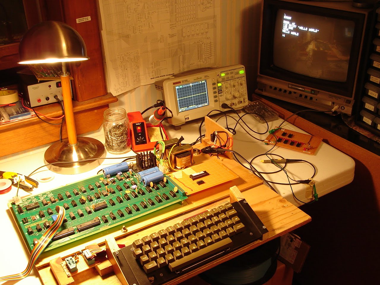
 Apple-1 (Mimeo) Clone with the BASIC firmware card attached, shows the BASIC up and running, Hello World!. After a 2+ hour debugging session with Mike Willegal's help, we determined that I had a bad connection at RAM location B-14 (X4) on pin 1. The oscilloscope image above shows the signal, (about 2 volts peak-to-peak split between + and - voltage levels) I had on pin 1. Pin 1 SHOULD show -5 volts.
This all started when I could not read the data I had just deposited into memory anywhere in Bank X. Mike had me test using 0 and FF at different memory locations, for example:
0:FF (deposit FF at mem location 0000)
0:0 (deposit 0 at mem location 0000)
1000:FF (deposit FF at mem location 1000)
1000:0 (deposit 0 at mem location 1000)
After doing the deposit, we checked the data with a read:
1000.1000
Output: 1F
What we were seeing was 5 bits that were"stuck" 0001 1 1 1 1
(wrong, this should have been 0 or 0000 0000 )
The next thing we did was swap the chip select jumpers:
Before:
W=>1
X=>0
After:
W=>0
X=> 1
Normally, the PROM monitor will use the X bank, so what we did here was to use the W bank of RAM instead. I switched the jumpers, and ran the tests again. Bank W was working correctly.
So this was a pretty good indicator that the problem was somewhere in the X bank and not somewhere else on the board. At this point, we started probing the ground and power pins at each X bank DRAM chip. I checked +5v (pin 9), +12v (pin 8) and lastly -5v (pin 1) until we found the problem.
UPDATE (June 18, 2010): Here is a test program Mike had me use for testing the RAM -
0: AD 00 10 4C 00 00
This HEX code is : LDA 1000 with a Jump back to 0
That will loop forever and generate an alternating square wave (toggling) on the oscillocope at pins 1 and 2
No comments:
Post a Comment